Circuit Diagram
The clap sensor is a simple circuit that incorporates a PC microphone, a microcontroller, and an output. The following diagram shows the logical circuit design:
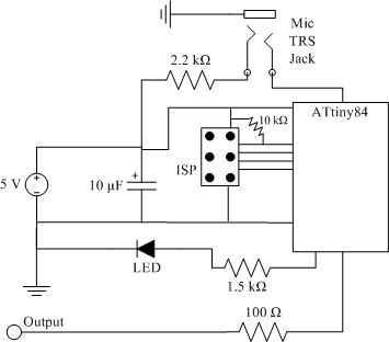
I chose the ATtiny84 microcontroller for this project because I’m familiar with the AVR architecture and I have access to the tools to use it. I bought the ATtiny84 in its SOIC-14 packaging. If I had it to do again then I’d choose the ATtiny85, which comes in a SOIC-8 package; it contains all the features I needed but takes up less space. It’s not a real problem though.
The microphone connects to the circuit through a tip-ring-sleeve (TRS) jack. I chose the SJ1-3533N jack from CUI Inc. because it looks nice and has a small footprint on the circuit board. It breaks out the tip, ring and sleeve conductors on three pins on the bottom. The sleeve conductor is connected to ground, and the ring is connected to V+ through a 2.2 kΩ resistor (without this resistor the microphone’s output signal is constant). The tip conductor carries the microphone’s output signal.
The circuit’s 10 μF capacitor filters the power input. The LED is for visual output. The LED’s current-limiting resistor value, in the diagram labeled 1.5 kΩ, depends on the LED. I used a low-current LED, so the resistance is quite high. The resistor value for other LEDs can be calculated with this tool, with the source voltage value set to the input voltage (5 V in my circuit) and the diode voltage and current taken from the LED’s datasheet.
I used a 100 Ω resistor to protect the output. The resistor should probably be higher, but I figure it’s fine.
Programming Interface
The six-pin connector next to the ATtiny84 in the circuit diagram is for the in-system programmer (ISP), which is how code is loaded onto the ATtiny84. I used Atmel’s AVRISP mkII to load code. The following diagram shows the ISP pinout on the header:
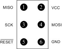
The ISP interface corresponds to a serial peripheral interface (SPI) connection; the only difference is that the microcontroller can be put into programming mode while the RESET pin is held low. This is all handled automatically by the AVRISP driver. The Vcc and GND pins have to be connected to external power. Also, the RESET pin must be connected to Vcc through a 10 kΩ pullup resistor as shown in the circuit diagram above, to keep RESET high when the processor is running. The header’s pins are connected to pins on the microcontroller. The microcontroller pins are labeled with their SPI (and RESET) designations in the microcontroller’s data sheet. For the ATtiny84, the datasheet [PDF] gives the pin designations on page 2:
| Name |
SOIC-14 Pin Number | AVR Pin Name |
| Vcc | 1 | Vcc |
| GND | 14 | GND |
| MISO | 8 | PA5 |
| MOSI | 7 | PA6 |
| SCK | 9 | PA4 |
| RESET | 4 | PB3 |
The AVRISP connects with the red stripe on its ribbon cable at the header’s pin 1.
Circuit Board Design
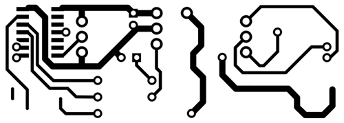
I designed the circuit board using a program called ExpressPCB. It’s not the most complete design program and it uses a proprietary file format that doesn’t work with other software, but it’s very easy to use and is well-documented. I designed the two-layer circuit board below; the red traces are the top copper layer, the green traces are the bottom copper layer, and the yellow is for silkscreened information (I don’t print the silkscreen layer, but it’s shown below for informational purposes).

The large holes fit standard 0.1″ headers; they have a 1.91 mm outer diameter and 1.02 mm inner diameter. The small holes fit component leads; they have a 1.42 mm outer diameter and a 0.74 mm inner diameter. The small holes on the CPU are just through-holes that connect the bottom layer copper to the top. The three resistor spots in the bottom-left corner of the board are sized for 1/4 W resistors.
The three 0.1″ pins in the upper-left corner are, from top to bottom, for V+, GND, and the output. The ISP header is oriented with pin 1 at the top-left.
This design doesn’t include the ISP port’s pullup resistor. I couldn’t figure out how to fit it onto the board. If I was going to make another version of the board I would put a surface-mount resistor between the Vcc and RESET pins to the right of the ISP port. I ended up using a 1/4 W resistor soldered above the board, between the Vcc trace and the through-hole connected to the RESET pin.
Etching the Circuit Board
I used instructions written by Christopher Garber to print the two copper layer designs onto toner transfer paper. I diverged from the instructions by printing to a 1200 dpi PDF file instead of 300 dpi; 1200 dpi gave me much better results for the final printing. I also skipped the colour-related steps and just printed everything to black, and combined the top and bottom layer images into one image for printing.
I also erased unconnected pads from the final printable image in Photoshop. Each through-hole has a pad on the top layer and a pad on the bottom layer, but most of them only connect to things on one layer. For example, the three left-most ISP header through-holes connect to traces on the bottom layer, but are unconnected on the top layer. I erased the top layer pads because they’re useless. In the lower part of the board the bottom-layer ground trace barely fits through two through-hole pads. By erasing the useless bottom layer through-hole pads, the risk of shorting the ground trace to the leads that fit through the holes is greatly reduced. I didn’t erase the bottom-left pad for the TRS jack, but I should have. (Design tip: I also caught a bug by erasing vestigial pads. When I erased the LED cathode pads on both the top and bottom layers, I discovered that I’d forgotten to connect the top layer pad to the ground trace.)
Finally I had the circuit ready to print to the toner transfer paper:
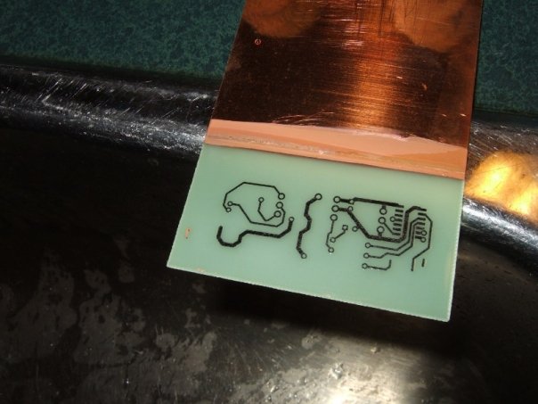
Note that the top layer is reversed to compensate for the toner transfer process. I bought materials for etching from a Chinese shop on eBay, but there are various other sources for the required products. I bought toner transfer paper, copper-clad PCBs, and copper etchant from Digole Digital Solution’s eBay store. I mostly followed their instructions, with supplemental information on cleaning, ironing and etching from Christopher Garber’s page. Mr. Garber uses high-gloss photo paper instead of toner transfer paper, but it seems way easier to use toner transfer paper since it transfers only the toner and doesn’t leave any residue that needs to be scrubbed off. Here is the copper-clad PCB after being cleaned and printed to:
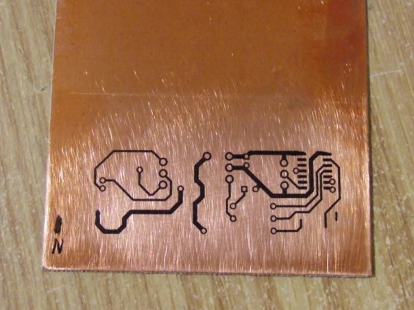
I also wrote the N and a line in black Sharpie ink to test how well the ink worked as an etch resist. I bought a double-sided PCB, but I ended up printing both of the circuit board’s layers to the same side because it seemed like too much hassle to line up the holes on the layers. I glued the layers together later. But before that I etched the copper in the etchant I bought from Digole:
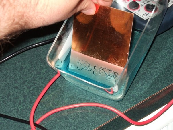
The Sharpie ink I drew on the PCB ended up getting washed off by the etchant. Fortunately after it started to run it got washed all the way off and didn’t cause streaks in the copper. I think if I had laid the PCB down instead of holding it up vertically then the ink would have stayed put. I was trying to save on etchant, but I ended up having to use extra anyway because it had to etch off both layers. After I was done I mixed in baking soda to precipitate out the copper ions, diluted the solution considerably, and dumped it down the sink. I think in the future I would use a solution of hydrochloric acid and hydrogen peroxide as an etchant, as recommended in various web sites, since it is easier to obtain and more environmentally friendly than whatever Digole was selling (I think I bought either sodium persulphate or ammonium persulphate, they don’t specify which). [note: I have since started using hydrochloric acid, and it is very effective. I will write more on that elsewhere on this site at some point.]
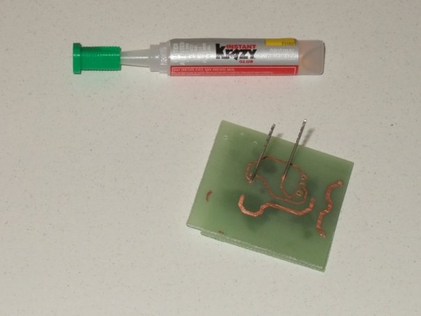
I washed the toner off with acetone and cut the circuit board out with a hacksaw. Then I drilled out the through holes with a drill press, using a #60 (1.01 mm) bit for the large holes and a #69 (0.74 mm) bit for the small holes. Not all of the through-holes were drilled out on both sides, because I had erased some of the through-hole pads from the printout and so they didn’t appear in the circuit board. The V+ pin and the CPU through-holes have pads on both sides, so those through-holes got drilled out all the way through. I glued the two pieces back-to-back, making sure they were properly aligned by pushing drill bits through two of the complete through-holes.
After letting the glue cure overnight I trimmed down the PCB’s edges using a rotary tool, and finished drilling all of the through-holes, leaving the final circuit board. The mic jack’s pins are very wide and narrow, so I carved them out with the small drill bit.
I installed the minimum number of components I needed to load code onto the microcontroller: the power input, filter capacitor, ISP header, pullup resistor, CPU, LED, and LED resistor. With this circuit I was able to read the CPU’s serial number using the AVRISP mkII, and finally to load a simple LED-blinking program.
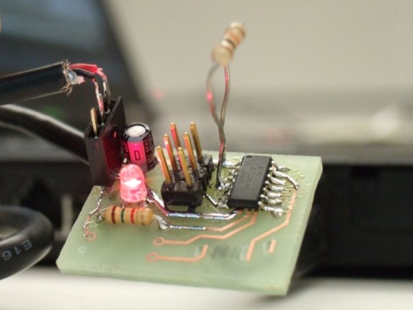
Soldering on the ISP header was very difficult because of the top layer pads: when the header was installed on the board, the pads were under the header and it was impossible to solder them to the pins. I solved this for the ISP header by putting a few metal strands from stranded-core wire into the holes. The strands wicked solder from the bottom of the board up to the pads. The strands are not easy to install and create a risk of short circuits. I solved this problem for the power, ground, and signal pins by removing the plastic base from the header row and soldering the pins into the holes one at a time. Later when I installed the TRS jack I came up with a better way to do it: drill through-holes next to the top layer pads, stick a bit of metal (e.g. a clipping from a component lead) through the hole, and solder the top layer pad to the metal. I soldered the TRS jack connectors to the bits of metal sticking out of the bottom layer, thereby connecting them to the top layer pads via the through-holes.
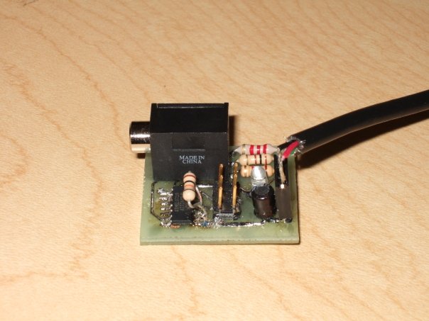
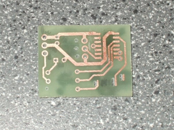
Finally I installed the remaining components and trimmed the pullup resistor. After I took the above photo I cleaned off the board and dipped it in polyurethane to protect the traces (this had the side-effect of making the board nice and shiney).