MiRF Package
The nRF24L01 radio controller is packaged on a MiRF-v2 board that includes a voltage regulator, 16 MHz oscillator, 8-pin breakout, external antenna connecter, and other electronic components. In this report I generally use the term “nRF24L01” to refer to the whole package of MiRF-v2 board and the actual nRF24L01 chip. There is a new version of the nRF24L01, called the nRF24L01+, which adds the ability to transmit at 250 Kbps as well as improved range and sensitivity; we use the original nRF24L01, although the driver code will also work on the + version.

nRF24L01 MiRF-v2 Landmarks
The MiRF-v2 board provides the following I/O pins:
- Vcc: 3.3V – 7V power input.
- CE: Chip Enable. This is brought low while loading data onto the radio or copying out a received packet, and brought high to set the radio to active receive/transmit mode.
- CSN: Chip Select N. This is the SPI slave select pin; it is brought low to initiate an SPI transaction, and brought high to complete the transaction.
- SCK: SPI Clock. The AT90 SPI module generates the clock signal automatically.
- MOSI: Master Out, Slave In. Data are transferred serially over this pin from the AT90 (master) to the nRF24L01 (slave). This pin is controlled automatically by the SPI module.
- MISO: Master In, Slave Out. Data are transferred serially over this pin from the nRF24L01 (slave) to the AT90 (master). This pin is controlled automatically by the SPI module.
- IRQ: Interrupt Request. The radio drives this pin low to trigger an interrupt.
- GND: Ground.
Wiring
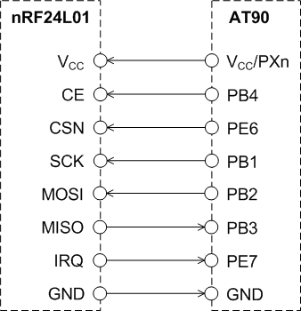
The following wiring diagram show the wiring between the radio breakout (left) and AT90 pins (right), ordered by the MiRF-v2 breakout. The arrows indicate data direction.:

nRF24L01 Wiring Diagram
The CE and CSN lines can be connected to any general output pin on the AT90 if PB4 and PE6 are unavailable. The IRQ line can be connected to any interrupt pin (INT0..7). Changing any of those pins will require changes to the software driver. The Vcc and GND lines can be connected to any of the AT90’s Vcc and GND pins without software changes, and the radio can be powered from a general I/O pin PXn (see the “Power Switch” section below). The SCK, MOSI, and MISO pins must be connected to the AT90 pins indicated above, because those pins are hardwired to the SPI module. I chose not to connect the nRF24L01’s SCN pin to the AT90’s SS pin, because the AT90’s SS pin could be used by some application to select the AT90 as a slave. In master-only mode, which is what the radio driver presented in this project assumes, the AT90’s SS pin does not have any special meaning.
Power Requirements
The following table shows the nRF24L01 chip’s supply voltage range (source: nRF24L01 Product Specification, page 13):
| Symbol | Parameter | Min. | Typ. | Max. | Units |
| Vdd | Supply voltage | 1.9 | 3.0 | 3.6 | V |
| Vdd | Supply voltage if input signals > 3.6 V | 2.7 | 3.0 | 3.3 | V |
| Temp | Operating temperature | -40 | +27 | +85 | ºC |
The MiRF-v2 board regulates the input to 3.3V; according to Bell (nRF24L01 tutorial 0, page 3), the MiRF-v2 can safely accept anywhere from 3.3V to 7V on Vcc. The AT90 produces 3.3V signals, and supplies 3.3V from the power pins that are available on each port, so the AT90 will interface with the radio within its specifications.
The radio draws a maximum of 12.3 mA when actively receiving a packet at 2 Mbps, and a minimum of 900 nA when in power-down mode. The current draw when transmitting depends on what the power output is configured to be, with a maximum of 11.3 mA when outputting at 1 mW. If the radio is not very busy then it will spend most of its time in a low-power standby mode waiting to receive a packet, in which it consumes 22 μA. See the nRF24L01 Product Specification, page 14, for more detailed electrical specifications. These currents fit well within the AT90 supply capabilities.
Range
The following table shows the radio’s transmitter output ability for the four configurable power settings, as well as the total current that the radio draws for each of the three settings:
| Power |
Signal Output | Total Current |
| 0 dBm | 1 mW | 11.3 mA |
| -6 dBm | 251 μW | 9.0 mA |
| -12 dBm | 63 μW | 7.5 mA |
| -18 dBm | 16 μW | 7.0 mA |
I estimate that two stationary radios can transmit packets successfully nearly 100% of the time at a range of 30 metres (all distances are line of sight), with the power set to 0 dBm and the transfer rate set to 1 Mbps on channel 112. Packets can get through about 25% of the time at a range of 100 metres, with the same settings. At -18 dBm and 2 Mbps, the radio’s maximum range is about 15 meters. The packet failure rate of the system seems to increase dramatically when the primary transmitter is moving (I assume the same thing happens when the primary receiver is moving, since both act as tranceivers during an Enhanced Shockburst™ transaction, but I have not tested this).
Power Switch
It is sometimes useful to disconnect the radio from power to reset its internal state. This can be done programmatically by connecting the nRF24L01’s Vcc pin to one of the AT90’s digital I/O pins instead of to the AT90’s Vcc pin. When the selected I/O pin, generally called PXn, is set high, the radio is powered on normally; but when it is driven low the radio powers down until the pin is set high again. PXn can safely supply up to 40 mA (see hardware specification [PDF], section 30.2), which is considerably more than the nRF24L01 draws. PXn must be toggled by the application to reset the radio; digital I/O pins do not necessarily change their values while the AT90 is being reset. If the AT90 loses power, e.g. by being unplugged, then the radio will also lose power.
Powering down the radio programatically is not necessary unless the user encounters a bug in the driver that leaves the radio in an unusable state. Normally, simply restarting the application (e.g. by resetting the AT90) should effectively reset the radio without powering it down. After the radio is powered down and power is re-applied, the radio must be reinitialized using the driver’s initialization routine.